Two-dimensional materials often have properties that differ from the corresponding bulk material. They can be useful, e.g., in electronics or optoelectronics. However, there is a lack of p-type semiconducting 2D materials. Existing examples of 2D p-type semiconductors often have drawbacks such as low carrier mobilities or a need for harmful chemicals in their synthesis.
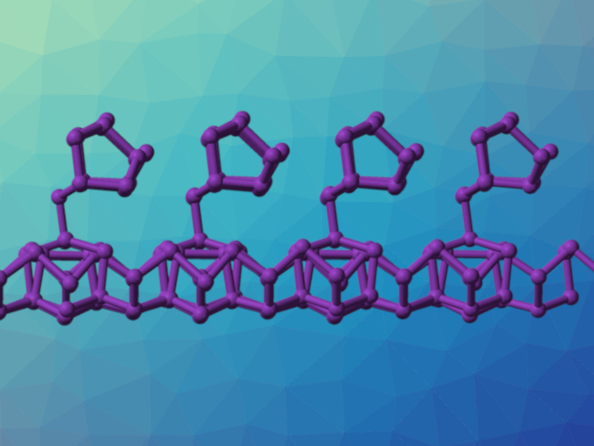
Paolo Samorì, University of Strasbourg, CNRS, France, and colleagues have developed a scalable, sonication-assisted, liquid-phase method for the exfoliation of violet phosphorus (VP, structure pictured) into few-layer-thick flakes. The team synthesized violet phosphorus via chemical vapor transport, using amorphous red phosphorus as a phosphorus source. Then they used N,N-dimethylformamide (DMF) as a solvent to disperse the violet phosphorus, followed by sonication for 5 h at 285 W to exfoliate the material.
The obtained violet phosphorus sheets were drop-cast to obtain thin films and used to build field-effect transistors (FETs) and a proof-of-concept complementary metal oxide semiconductor (CMOS) circuit element. The researchers found that the material could be a useful p-type 2D semiconductor for (opto)electronic applications.
- Two-Dimensional Violet Phosphorus: A p-Type Semiconductor for (Opto)electronics,
Antonio Gaetano Ricciardulli, Ye Wang, Sheng Yang, Paolo Samorì,
J. Am. Chem. Soc. 2022.
https://doi.org/10.1021/jacs.1c12931


